Physics of novel materials with silicon for advanced detector applications (SWIR)
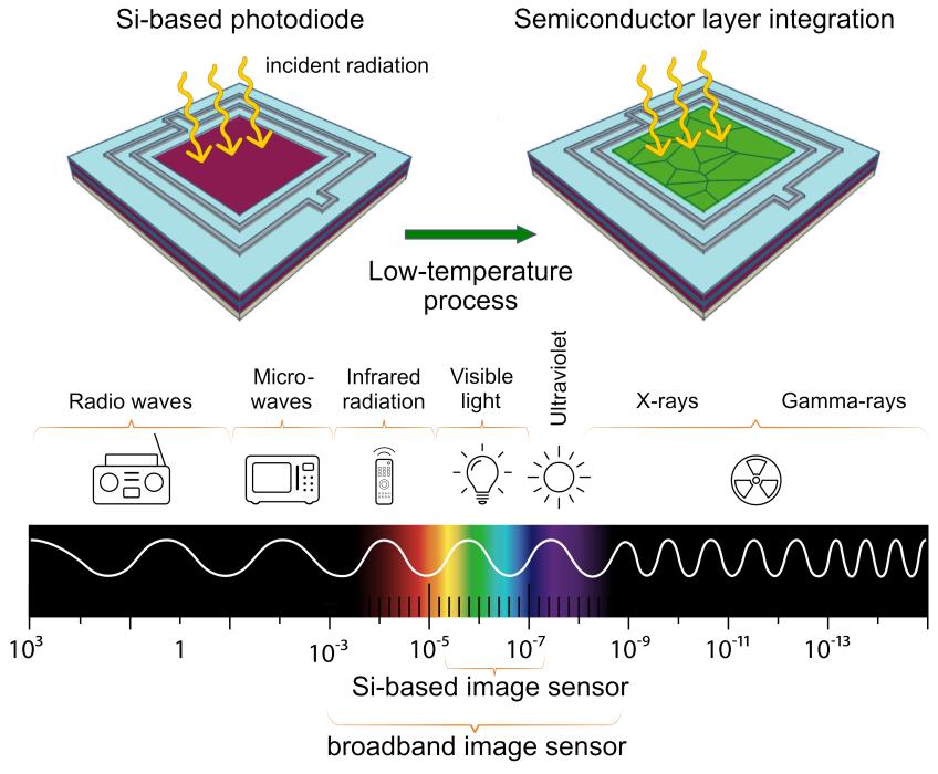
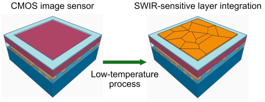
The demand for broadband image sensors capable of sensing diverse radiation types, e.g., electrons, photons, and high-energy particles, is continuously growing. The best solution would be to realize these sensors using CMOS technology to leverage its advantages in tighter integration and scalability. However, silicon has a limited absorption range from the visible to the near-infrared spectrum (400 nm - 1100 nm), making it unsuitable for detecting radiation outside the visible and near-infrared range. This project seeks to address these limitations by integrating various semiconductor materials and compounds, such as germanium, III-V, II-VI, and other novel materials, with silicon through low-temperature (≤ 350 °C), CMOS compatible processes.
The primary goal of this research is to investigate the interface physics between these semiconductor materials and silicon at low temperatures while identifying the optimal process conditions to realize highly efficient detectors capable of sensing various radiation types. Then, fabrication and experimental analysis of test structures will be performed to validate the practical viability of the process and provide recommendations for further development and optimization. The expected outcome is an advance in the field of radiation detection by enabling the creation of highly efficient broadband image sensors
Project data
| Starting date: | November -0001 |
|---|---|
| Closing date: | November -0001 |
| Contact: | Padmakumar Rao |